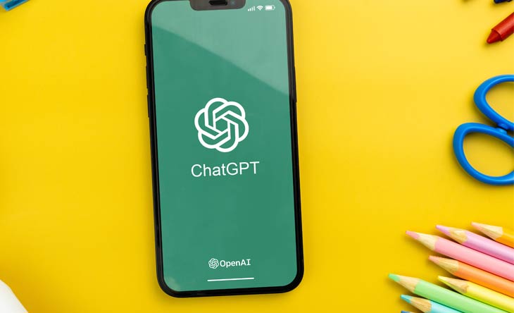
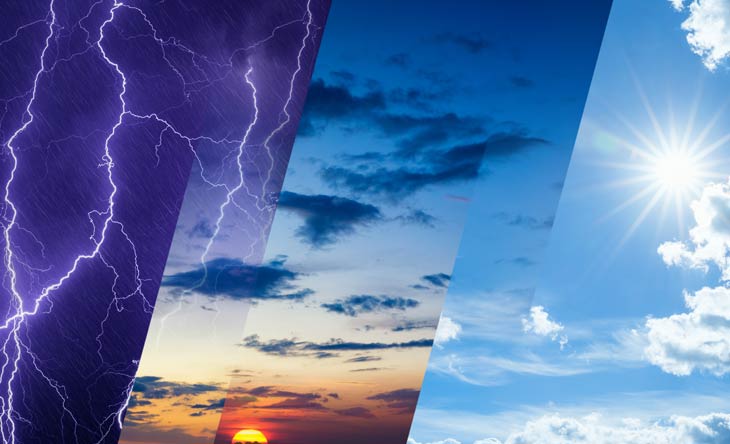
You can find it here: http://ascii.jp/elem/000/000/489/489200/ (in Japanese, translations: Google, Babelfish - you have to read it a bit like Master Yoda due to the different syntax of the Japanese language)
While this article again mentions a shared L1 instruction cache, Johan de Gelas already confirmed dedicated instruction caches for the two threads executed by a Bulldozer module. Also CVT16 already vanished from AMD documents and seems not to be supported anymore or at least not in Bulldozer. There are also some small errors in the description of the behaviour of older and current microarchitectures. To me it also seems, that there has been some influence by Hiroshige Goto's articles.
Further it has a schematic view of the Bulldozer microarchitecture with :

This is interesting (also for those not reading the translations), as it introduces additional decode and schedule stages in the integer cores. The author has some interesting thoughts.
But the best information is this one (quoted from both linked machine translations):
"However, this is about Japan from AMD AMD over the U.S., clearly 'the two per thread ALU, AGU is one of four the total of 2', the answer that came back."
or
"However, in regard to this by way of Japanese AMD the United States AMD compared to, clearly, 'per thread ALU two, AGU two is totals four', you questioned and detour answer returned."
This looks like an official confirmation for an integer core having 2 ALUs and 2 AGUs. So I don't need to change my old schematic views of the modules' microarchitecture in this regard. You'll remember (or read), that after the Financial Analyst Day I thought, that there might be more integer power.
During the last week I have found a good explanation (at least satisfying for me), which is clearly different to that of the articles' author. More on that soon.

Leave a comment